
Manufacturing, Testing & Quality
A 24 V supply can overshoot at the board: choosing damping, clamping and controlled startup
Summary: A board can see a voltage above the supply setting when an already energized cable is connected. Before increasing the input capacitor or adding a TVS, separate two jobs: controlling the voltage at the board's input and controlling the charging current into its downstream load. The protection must act at the node that needs it.
This Application Note is for an electrical or integration engineer reviewing a cable-fed 24 V input before a cable, capacitor or power-path change. It provides a mechanism, a comparison of protection approaches and a bounded way to prepare an evaluation. The worked model is an illustration, not a component selection or a measured assembly result.
Follow the energy to the input capacitor
Cable inductance resists a sudden change in current. When a charged source first supplies an uncharged input capacitor, current builds through that inductance. Reaching the source voltage does not instantly stop the current: energy stored in the inductance can continue charging the capacitor above that voltage. Resistance dissipates energy and reduces the oscillation. The relevant circuit includes the source, cable, connector, input capacitance and the load’s startup behavior.
Analog Devices’ AN88 demonstrates why a nominal supply label is insufficient. Its March 2001 example used a 24 V source; Table 1 reports a 57.2 V peak with 1 uH and a 10 uF ceramic input capacitor. That is one documented setup, not a prediction for another cable assembly. It also shows why “twice the supply” must not become a system-wide upper bound. AN88, pp. 1-2
An ideal linear model helps explain the mechanism without pretending to predict every peak. Take a step source, series inductance L and resistance R, and an initially uncharged, fixed capacitor C. Exclude a load, contact bounce, source regulation and protection devices. The capacitor voltage follows:
L C d2v/dt2 + R C dv/dt + v = Vs
With zero resistance, v(t) = Vs [1 - cos(t / sqrt(L C))]. Its first peak is 2 Vs at pi sqrt(L C). This is a result of those assumptions. A real input can violate them. For the damped series model, the damping ratio is zeta = (R / 2) sqrt(C / L).
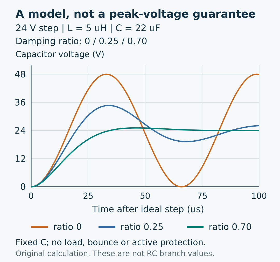
For an illustrative 24 V step, L = 5 uH and C = 22 uF, the lossless model’s first peak is 48 V at about 33 us. Adding damping reduces the modeled peak. The curves compare damping ratios of 0, 0.25 and 0.70 with every other model input unchanged. They do not specify an RC snubber: adding a separate RC branch changes the circuit and requires its own model.
The curve data (CSV) lets you reproduce this illustration. All rows are calculated model samples, not measured waveforms.
The practical implication is to review the changed system, not just the replacement part’s nominal value. A cable change changes impedance; a capacitor change changes capacitance and losses. The source and load may also change during the event. A calculation using one constant C cannot establish what a voltage-dependent capacitor will do.
Three approaches, three different jobs
The comparison below is an engineering synthesis of the cited design material. The approaches can be combined when the same input needs more than one function.
Scroll tables horizontally to read every column.
| Approach | What it acts on | A useful starting condition | What still needs evaluation |
|---|---|---|---|
| Damping branch: a resistor in series with an additional capacitor, connected across the input | Oscillating energy at the input | The main concern is ringing after connection to a reasonably steady DC source | Branch values, capacitor behavior, resistor pulse stress and interaction with the input filter |
| TVS clamp across the protected node | Voltage excursions that drive the device into conduction | A workable voltage window exists between maximum normal voltage and the protected circuit’s limit | Actual clamp voltage at the event current, tolerance, temperature, pulse energy, repetition and connection inductance |
| Hot-swap controller or eFuse with controlled output slew | Charging of capacitance downstream of its pass element | Startup current, supply sag or load sequencing also needs control | Input-pin exposure, output ramp under load, pass-element stress, thermal behavior and fault/retry behavior |
Damping: keep the main decoupling job intact
TI’s SLUAAL8 distinguishes the IC’s local input capacitor from an added series-RC branch. The branch connects across the input; its resistor is not inserted into the main DC supply path. That distinction matters when low impedance is needed for the converter’s normal switching current. Its example values belong to a particular charger input, so they should not be copied into an arbitrary 24 V design. SLUAAL8, Section 3
A useful candidate therefore starts with the existing input requirements intact and adds an explicitly modeled loss path. Evaluate the added branch with the actual range of cable and source impedance. “More capacitance” alone does not specify the damping, and the name “electrolytic” does not establish a particular ESR.
Pulse survival is a separate check. TI’s 2025 hot-plug discussion describes damping resistors that failed despite apparently adequate steady-state sizing. The resistor’s pulse curve and the actual event shape matter as well as average dissipation. TI, “Hot plugging DC/DC converters safely”
Clamping: use a voltage window, not the part’s headline voltage
A TVS has a working standoff voltage, a breakdown region and a clamping voltage at specified current. These are different points on its characteristic. SLUAAL8 uses that distinction when discussing selection. SLUAAL8, Section 4
For a proposed part, compare the maximum normal voltage with its allowable standoff behavior. Then compare its relevant clamp characteristic, including the connection path, with the protected input’s approved transient limit. If those requirements leave no usable margin, choosing a part merely because it says “24 V” does not solve the problem. Reconsider the protection architecture or the downstream rating. A clamp also needs a defined energy and repetition duty; clipping a waveform is not evidence that repeated events are acceptable.
Controlled startup: locate both sides of the pass element
Output slew control spreads capacitor charging over time. For a linear ramp, the capacitor contribution is Icap = Cout x dVout/dt; any active load adds current. As an original arithmetic example, charging 470 uF from 0 to 24 V in 20 ms requires an average capacitive current of 0.564 A. A hypothetical constant 0.2 A load would bring the total to about 0.764 A. This is not a setting recommendation: a real load may have a different startup profile.
The TPS2663 Rev. G data sheet describes adjustable output slew and thermal regulation that can alter charging behavior. Its input transient-protection and layout guidance remains relevant even when output startup is controlled. TPS2663, Sections 8.3.1, 9.5.1 and 9.6 TI’s separate SLVAEB9A startup comparison explains why limiting current alone can still leave a power switch with enough thermal stress to interrupt startup.
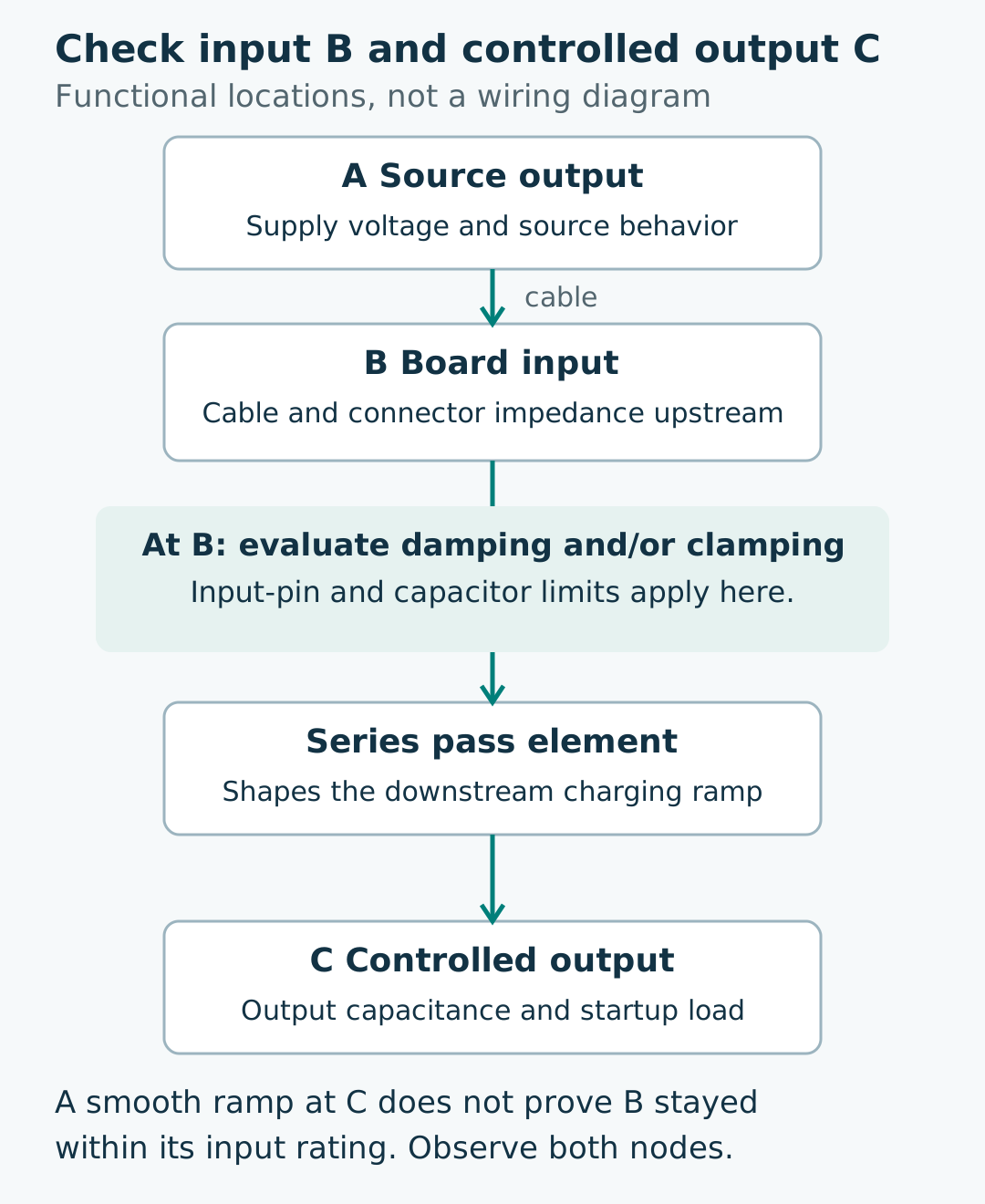
A smooth ramp at C does not prove that B stayed within its input rating. The same distinction applies to a converter whose output has soft start: establish what happens at its input rather than inferring it from the output trace.
Prepare an evaluation that can change the decision
Begin with the intended connection procedure. If the equipment requires power-off connection, retain that procedure. A protection study does not grant permission to hot-plug a connector or operating machine. Any energized-transient work belongs in an approved, energy-limited test fixture under the responsible electrical engineer’s procedure, not an improvised field reconnection.
Before selecting candidate components, prepare a compact input definition: source voltage range and behavior, cable and connector variants, input-capacitor part and relevant operating conditions, load startup, and the maximum permitted voltage at each exposed node. Separate the normal operating limit from absolute maximum ratings and any explicitly specified transient allowance. An absolute maximum is not a target waveform.
Use this decision sequence:
- Identify the exposed node. Mark the board input, any protection IC input and the controlled output. Define a measurement for each node whose rating could decide the design.
- Choose the missing function. Ringing suggests evaluating damping; insufficient voltage margin suggests evaluating clamping or a different architecture; excessive charging current or supply sag suggests evaluating controlled startup. More than one can apply.
- Review the candidate before energizing. Check voltage and pulse stress, load behavior and the source/fixture limits. Resolve an unbounded stress estimate before a hardware trial.
- Compare at the component terminals. Retain the actual trace, voltage/current reference, probe arrangement, bandwidth and operating conditions. A reading at the supply terminals cannot substitute for the board input. Have the test owner check whether the probe loop or grounding changes the observed event.
- Close on limits, not appearance. A smaller peak is useful only if every affected node and protection component satisfies its predeclared electrical and thermal limits, including the intended repetition and recovery behavior. Stop an evaluation on exceeded limits, unexpected heating, protection cycling or a measurement that cannot be interpreted.
The outcome can be a selected architecture for further qualification, or a precise missing input: for example, no documented clamp margin at the expected current, or an unknown startup load. One clean waveform does not qualify a cable family, a component substitution or a production assembly.
If cable or connector resistance is one of the uncertain inputs, continue with Low-resistance connector measurements. It explains how to define the measured path before comparing readings. A DC resistance measurement does not establish cable inductance or transient immunity.
Materials for the next design review
The primary documents below provide mechanisms and implementation examples. They are manufacturer material, not measurements of an MTTJ assembly. AN88 is historical technical evidence; its old component examples do not establish present availability.
- Analog Devices AN88, March 2001: the documented transient example and damping comparisons.
- TI SLUAAL8, May 2023: input model, additional RC branch and TVS characteristic.
- TI, “Hot plugging DC/DC converters safely,” September 2025: pulse-stress pitfalls in a different, higher-voltage example.
- TPS2663 data sheet, Rev. G, June 2024 and current product resources: an industrial eFuse example, evaluation-board documentation and design resources. Resource availability does not establish stock or suitability for a particular assembly.
- TI SLVAEB9A, February 2022 revision: a comparison of constant-current, constant-power and thermally regulated startup approaches.
Sources checked 26 October 2026. AI-assisted research and original explanatory diagrams. No MTTJ bench result is presented.
Related resources and manufacturing scope
- Low‑resistance connector measurements: what four‑wire sensing, dry‑circuit conditions and offset compensation each address
- Shield termination at one end or both: first check frequency, equipotential bonding and the termination path
- Single‑pair Ethernet and power: approach selection, bench structure and evaluation preparation